MIT Builds AI Model That Detects Six Types of Atomic Defects in Materials Without Cutting Them Open
The machine learning system, trained on 2,000 semiconductor materials covering 56 elements, uses neutron-scattering data to noninvasively identify defects that could improve heat transfer and energy conversion.
Researchers at MIT have developed a machine learning model that can classify and quantify atomic defects in semiconductor materials using noninvasive neutron-scattering data — a breakthrough that could reshape how engineers design everything from solar cells to thermoelectric generators. The system was trained on a computational database of 2,000 semiconductor materials spanning 56 elements in the periodic table.
The Problem With Point Defects
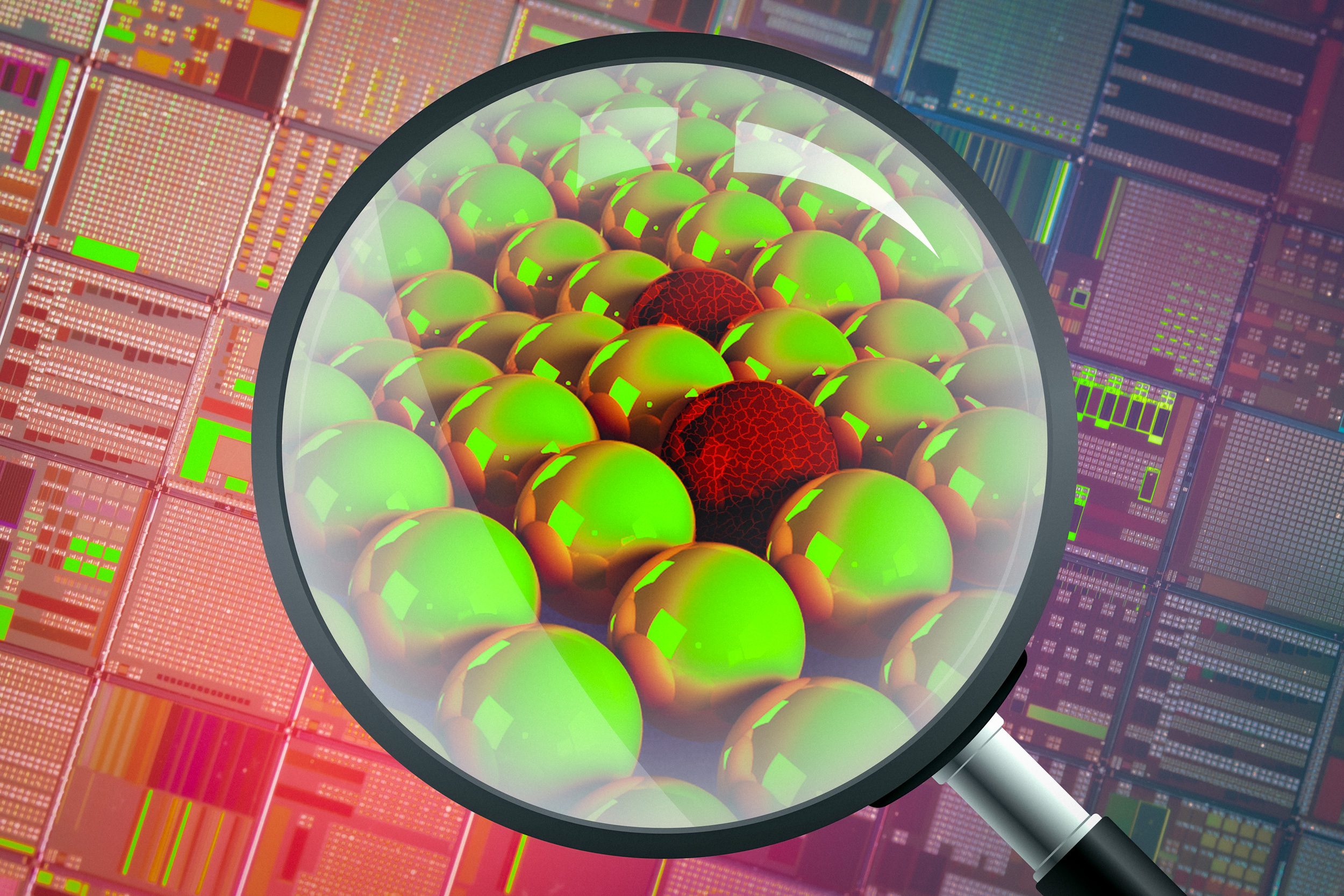
Point defects — places where atoms are missing, displaced, or substituted within a crystal lattice — play an outsized role in determining a material's properties. A single vacancy or interstitial atom can dramatically alter how a semiconductor conducts heat, converts energy, or withstands mechanical stress. Yet measuring these defects has historically required destructive techniques that damage or destroy the very samples being studied.
Conventional methods like transmission electron microscopy can visualize individual defects, but they require slicing materials into ultra-thin samples and can only examine small regions at a time. For bulk materials used in real-world applications, this limitation makes comprehensive defect characterization impractical.
A Multihead Attention Approach
The MIT team's solution leverages the same multihead attention mechanism that underpins large language models like ChatGPT, adapted for an entirely different domain. Instead of processing text tokens, the model analyzes vibrational frequency data obtained from neutron-scattering experiments.
The approach works by comparing paired samples — one doped (intentionally modified) and one undoped — and analyzing the differences in their neutron-scattering signatures. These vibrational fingerprints encode information about the type, concentration, and configuration of point defects present in the material.
What makes the system particularly powerful is its ability to detect up to six distinct types of point defects simultaneously within a single sample. This multidefect detection capability is something that no conventional technique can achieve noninvasively.
Scope and Training
The model's training dataset covers an unusually broad swath of the periodic table. By encompassing 56 elements across 2,000 semiconductor compounds, the system can generalize across material families — from traditional silicon-based semiconductors to emerging compounds used in next-generation energy technologies.
The researchers designed the training pipeline around computationally generated neutron-scattering spectra, allowing them to build a dataset far larger than what would be feasible through physical experiments alone. Each simulated sample includes known defect configurations, giving the model precise ground-truth labels to learn from.
Applications in Energy and Manufacturing
The practical implications extend across multiple industries. In renewable energy, understanding and controlling point defects is critical for optimizing the efficiency of solar cells and thermoelectric devices that convert waste heat into electricity. Defect engineering — deliberately introducing specific defects to tune material properties — is a growing field, but it depends on the ability to measure outcomes accurately.
For semiconductor manufacturing, noninvasive defect detection could enable quality control at scale, identifying problematic batches before they reach downstream fabrication steps. The system could also accelerate materials discovery by allowing researchers to rapidly screen candidate compounds for desirable defect profiles.
What Comes Next
The team is working to validate the model against experimental neutron-scattering data from real materials, moving beyond the computationally generated spectra used in training. If the approach transfers successfully to physical measurements, it would represent a significant step toward deploying AI-driven materials characterization in industrial settings.
The research also highlights an emerging pattern in scientific AI: applying architectures originally developed for natural language processing to structured physical data, where the "grammar" of atomic vibrations encodes information just as syntax encodes meaning in text.
Newsletter
Get Lanceum in your inbox
Weekly insights on AI and technology in Asia.